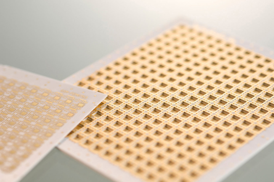
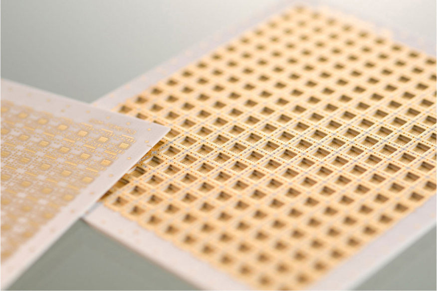
LTCC Multilayer Substrates(NL-Ag3)
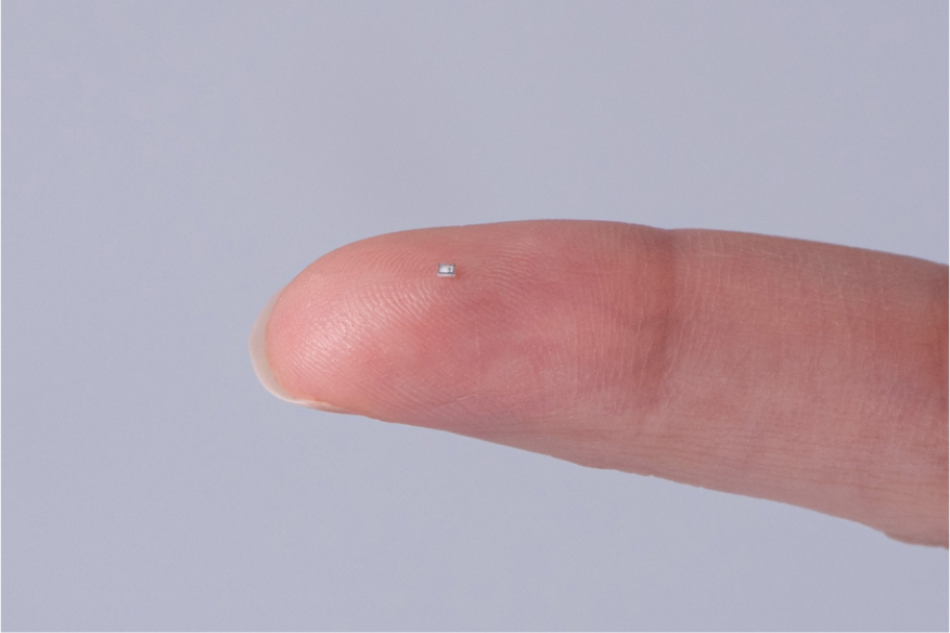
The NIKKO LTCC substrates with Ag conductor material offer a multilayer substrate with low dielectric loss. Coils, capacitors, and resistors can be embedded in the internal layers. Ideal for high-frequency modules and silicon wafers interposer substrates.
Features
The NIKKO LTCC substrates can have embedded coils, capacitors, and resistors that allow reducing substrate size. Excellent dimensional tolerance of ±0.3% provides improves mounting accuracy. Low conductor loss is achieved by using Ag conductor material. Electroless Ni/Au plating or Electroless Ni/Pd/Au plating are available for surface treatment.
Material Characteristics
| ITEM | UNIT | TEST CONDITIONS | NL-Ag3 | NL-Ag8 |
|---|---|---|---|---|
| COLOR | ― | ― | WHITE | WHITE |
| DENSITY | g/cm3 | ― | 2.85 | 3.2 |
| BENDING STRENGTH | MPa | ― | 250 | 370 |
| THERMAL EXPANSION | 10-6/K | RT~350℃ | 5.5 | 10 |
| THERMAL CONDUCTIVIT | W/(m・K) | ― | 3.5 | 2.7 |
| DIELECTRIC | ― | 10GHz | 6.9 | 6.7 |
| 20GHz | ― | 6.7 | ||
| 40GHz | ― | 6.7 | ||
| 80GHz | ― | 6.7 | ||
| 100GHz | ― | 6.7 | ||
| LOSS TANGENT | 10-4 | 10GHz | 60 | 4 |
| 20GHz | ― | 8 | ||
| 40GHz | ― | 12 | ||
| 80GHz | ― | 16 | ||
| 100GHz | ― | 19 |
Design Guidelines
| ITEM | UNIT | STANDARD | CUSTOM | |
|---|---|---|---|---|
| DIMENSIONS | inch | 2~4 | ー | |
| TOLERANCE | % | ±0.35 | ー | |
| THICKNESS TOLERANCE | % | ±10 | ー | |
| # OF LAYERS | Layer | 2~ | ー | |
| VIA DIAMETER | mm | 0.15, 0.2 | 0.1 | 0.085 |
| VIA PAD DIAMETER | mm | VIA DIAMETER +0.15 | VIA DIAMETER +0.1 | VIA DIAMETER +0.05 |
| VIA PICTH | mm | 0.5 | 0.35 | 0.25 |
| LINE/SPACE | mm | 0.1/0.1, 0.15/0.15 | 0.075/0.075 | |
| LINE/VIA PAD DISTANCE | mm | 0.2 | 0.1 | |
| VIA EDGE/SUBSTRATE EDGE DISTANCE | mm | 0.5 | 0.25 | |
| LINE/SUBSTRATE EDGE DISTANCE | mm | 0.3 | 0.15 | |
| CAVITY WALL WIDTH | mm | ≧0.5 | 0.35 | |
| CAVITY DEPTH | mm | LESS THAN 2/3 OF TOTAL THICKNESS | ー | |
| CAVITY CORNER R | mm | 0.15, 0.2 | 0.1 | |
| CAVITY BOTTOM THICKNESS | mm | ≧0.3 | ー | |
Electroless Ni/Au plating or Electroless Ni/Pd/Au plating
※Please inquire about designs other than those mentioned above
Catalog Download
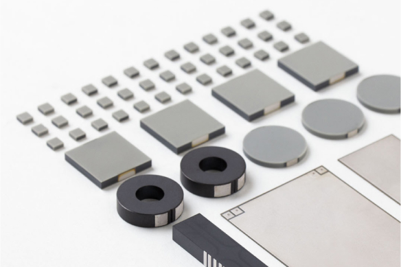
Product Use Cases
- High-Frequency application substrates(Front-end modules, Sensor substrates)
- Substrates for small package devices
- Silicon wafer interposer substrates
Find Products
Free consultation with easy form that only takes 90 seconds
Feel free to contact us to ask about our products and services.
