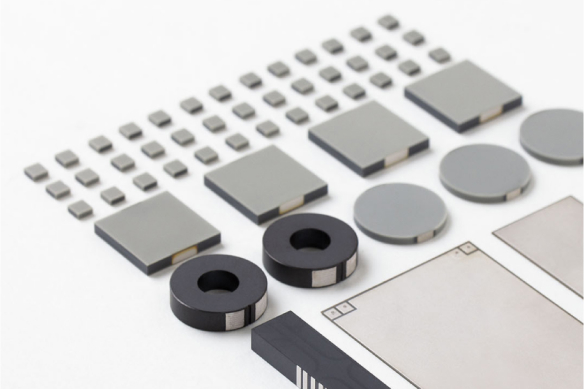
Thick Film Printed Circuit Substrates
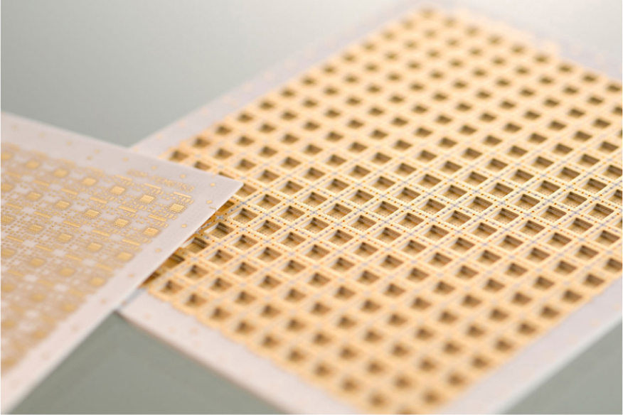
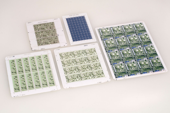
These printed thick film circuit substrates are ceramic circuit board substrates with printed metal conductors, resistors, and overcoat glass printed on NIKKO ceramic substrates. Via filled substrates with through holes filled with Ag metal conductor material are also available. The use of NIKKO’s in-house ceramic substrates provides an end-to-end solution from design to the final product.
PRODUCT LINEUP
Substrates: 96% Alumina, Alumina-Zirconia
Conductors: AgPt, AgPd, Cu, Au
※Materials that comply with ROHS II are also available
Features
By utilizing NIKKO’s in-house substrates as the base substrate, these substrates offer not only excellent thermal conductivity but also high reflectivity and insulation. Available in a wide range of substrate sizes and circuit patterns along with the capability of high-density circuits with fine patterns.
With the via-filled substrates, pads on via are available for small high-density circuits. The filled vias can also be used as thermal vias for Chip on Board assemblies and surface mount devices that require thermal dissipation. Thick film resistors can be printed and trimmed for resistance tolerances from ±1%, allowing for reduction of surface mount devices to achieve smaller, high-density circuit boards. Trimming also allows for producing the required resistance values.
Material Characteristics
| ITEM | UNIT | VALUES | ||
|---|---|---|---|---|
| CONDUCTOR | TRACE RESISTANCE | AgPd | μΩ・cm | <50.0 |
| AgPt Au | <5.0 | |||
| RESISTER | RESISTOR MATERIAL RESISTANCE RANGE | AgPd | Ω/□ | 0.1~1.0 |
| RuO2 | 1.0~1M | |||
| TCR | AgPd | ppm/℃ (25~85℃) | 0±100 | |
| RuO2 | 0±150 1~100kΩ/□ | |||
| 0±300 1MΩ/□ | ||||
| INSULATION | INSULATION RESISTANCE | 100VDC | MΩ | ≧10000 |
| WITHSTANDING VOLTAGE | DC、at25μm | V | ≧500 | |
| VIA CONDUCTOR | CONDUCTOR RESISTIVITY | AgPd | μΩ・cm | 120 |
| THERMAL CONDUCTIVITY | W/(m・K) | 53.0 | ||
Design Guidelines
| ITEM | STANDARD | CONDITIONS | ||
|---|---|---|---|---|
| THICKNESS | mm | 0.635 | 1.0 | ― |
| DIMENSIONS | mm | 114.3×94.7 106mm□ OTHER AVAILABLE | ― | |
| CAMBER | mm | LESS THAN 0.25 | WITH 106mm□ | |
| VIA DIAMETER | mm | LESS THAN Φ0.3 | ― | |
| PAD DIAMETER | mm | LESS THAN Φ0.7 | ― | |
| LINE/SPACE | μm | MORE THAN 150/150 | ― | |
Plating Options
- Electroless Ni/Au plating or Electroless
- Ni/Pd/Au plating
Product Use Cases
- LED Lighting applications
- Automotive applications
- Hybrid IC (HIC) applications
- Industrial applications
