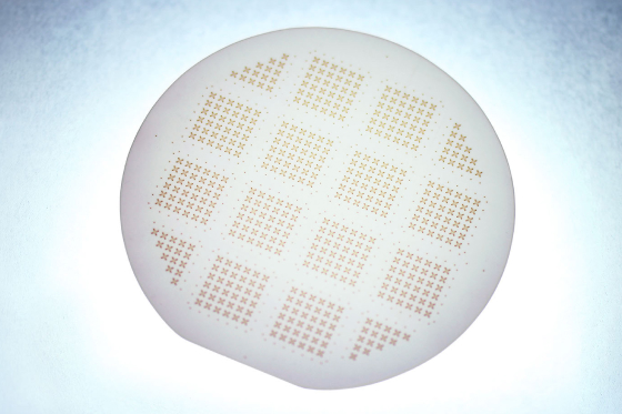
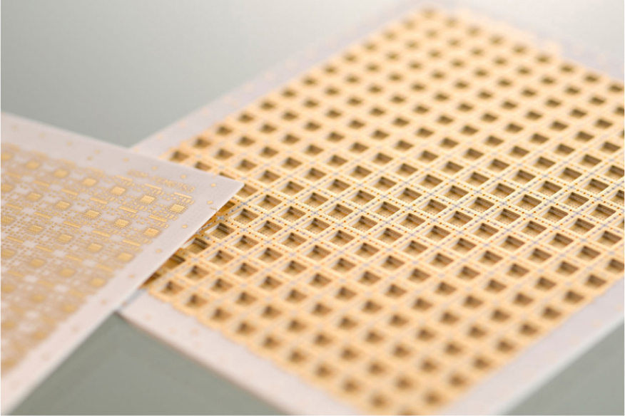
Product Wafer Level Packaging Substrates
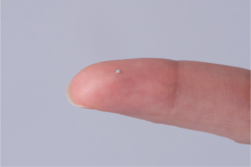
The thermal expansion coefficient of these LTCC substrates is adjusted for use as Wafer Level Packaging substrates. The substrate surface has bumps for electrical connectivity and by bonding directly to silicon wafers, allows for easy assembly of CSP (Chip Scale Packaging). Ideal for MEMS and semiconductor ceramic packages with a small number of leads.
Features
Benefits of using a ceramic wafer capable of anodic bonding with silicon
- Miniature,low profile,light weight devices become available
- Lower cost with higher units per wafer count and simple assembly process
- Faster development stage without the designing of electrical contacts
Hermetic sealed packaging technology with electrical connections (Etched Via Wafer)
※Products using this assembly technology will require a license aagreement with Tohoku University.
Material Characteristics
| ITEM | UNIT | TEST CONDITIONS | VALUES |
|---|---|---|---|
| DENSITY | g/cm3 | ― | 2.43 |
| THERMAL EXPANSION COEFFICIENT | ppm/℃ | ― | 3.4 |
| BENDING STRENGTH | MPa | POST-FIRING | 150 |
| POST-POLISH | 220 | ||
| YOUNG MODULUS | GPa | ― | 81 |
| POISSON COEFFICIENT | ― | ― | 0.23 |
| THERMAL CONDUCTIVITY | W/(m・K) | ― | 1.67 |
| INSULATION RESISTANCE | Ω・cm | 31℃ 500VDC | 6.5×10¹² |
| DIELECTRIC CONSTANT | ― | 1MHz | 5.4 |
| 10GHz | 5.1 | ||
| DIELECTRIC LOSS | ― | 1MHz | 0.01 |
| 10GHz | 0.01 |
Design Guidelines
| ITEM | STANDARD | CUSTOM | |
|---|---|---|---|
| LAYER THICKNESS | mm | 0.07(0.05~0.07) | 0.05(0.035~0.05) |
| MAX DIMENSIONS | inch | Φ4 | Φ6 |
| MIN THICKNESS | mm | 0.25 @3inch 0.3 @4inch | 0.25 @3inch 0.3 @4inch 0.4 @6inch |
| CAVITY DEPTH | mm | 0.025(0.003~0.05) | 0.025(0.003~0.05) |
| # OF LAYERS | Layer | MULTILAYER CIRCUITS AVAILABLE | MULTILAYER CIRCUITS AVAILABLE |
| VIA POSITION TOLERANCE | μm | 4 inch WAFER:±135 | MEMS SIDE : STANDARD±50 PREMIUM±35 |
| 0.2% OF WAFER RADIUS +35 | TERMINAL SIDE: ±50 | ||
| VIA DIAMETER | mm | 0.1±0.03 | 0.11±0.03 |
| MIN VIA PICTH | mm | 0.25 | 0.25 |
| MIN VIA PITCH (ETCHED VIA BUMP) | mm | 0.3 | 0.3 |
| MIN INTERNAL VIA PAD DIAMETER | mm | 0.15 | 0.15 |
| MIN LINE WIDTH | mm | 0.075 | 0.075 |
| MIN LINE SPACE | mm | 0.075 | 0.075 |
| MIN LINE/VIA PAD DISTANCE | mm | 0.1 | 0.1 |
| MIN VIA EDGE/CAVITY EDGE DISTANCE | mm | 0.2 | 0.2 |
| MIN VIA EDGE/SUBSTRATE EDGE DISTANCE | mm | 0.2 | 0.2 |
| MIN LINE SUBSTRATE EDGE DISTANCE | mm | 0.15 | 0.15 |
Catalog Download
Product Use Cases
- MEMS and semiconductor ceramic packages with a small number of leads.
Find Products
Free consultation with easy form that only takes 90 seconds
Feel free to contact us to ask about our products and services.
